Complicated Assembly Services from Silitronics team with
100+ years Hands On Process Development Experience

Microelectronics Assembly Capabilities

Flip Chip

  • Flip Chip +/- 2um placement
  • Active Alignment +/-0.5um
  • Die Attach: Eutectic & Epoxy
  • Chip on Board + Flex
  • Thermocompression Flip Chip
  • Thermosonic Flip Chip

Wire Bonding

  • Gold (0.7mil to 2.0mil)
  • Aluminum (1mil to 15mil)
  • Stud Bumping for Flip Chip
  • Wedge, Ball and Stich
  • Ribbon for RF + mmIC + GaN
  • Controlled loop height + length

SiP PCBA

  • Expertise on Complex SiP
  • PCBA with bare ICs
  • FR-4, Flex and Ceramic
  • SMT Assembly on both sides
  • Automatic Pick & Placement
  • BOM Management

Flip Chip

Verify Bump Quality + Height

Verify Bump Quality + Height

Flip Chip + 900 Cu Pillars

Flip Chip + 900 Cu Pillars

X-ray, Test, X-section

X-ray, Test, X-section

Flip Chip on
Ceramic 30GHz

Flip Chip on
Ceramic 30GHz

23x23 670FCBGA with 2000 SAC305 Bumps

23x23 670FCBGA with 2000 SAC305 Bumps

Gold Stud Flip Chip for Silicon Photonics

Gold Stud Flip Chip for Silicon Photonics

Chiplet Hetrogeneous Integration

The chip integration with Silicon Interposer is in its initial stage as customers want to have flexibility to select chips with different packages. The main advantages are to save on cost, size, power and cycle time without sacrificing performance and quality. Contact Silitronics team to discuss your specific applications.

SiP carrier substrate provides a platform for multiple chips or packages or passive components assembly. The applications include Multi-Chip Module (MCM), Multi-Chip Package (MCP), Stack Die, Package in Package (PiP) and Embedded Substrates. SiP integrates inhomogeneous ICs and other components with compact profile and faster time-to-market.

MultiChip Module (MCM)

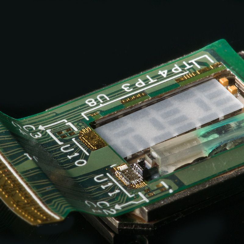
System in a Package (SiP)

SiP RF Module

Chiplets - Heterogeneous Integration

Key takeaways SiP Chiplet Integration

  • Layout of Substrate or Boards to integrate Chips or Pre-Packaged boards
  • Behavioral Modeling of the Chiplets for system level verification
  • SI/PI + DFA/DFM optimization to get the best performance and lowest cost
  • Full turnkey services from layout to prototype to volume
  • Great understanding of Chip layout which enables Silitronics team to offer the most optimized layout and assembly solutions

Wire Bonding

SiP Multi Tier Fine Pitch with Deep Access Long Wires

Six Tiers Wire Bonding with Fine Pitch

Complex SiP Module, 5 Tiers, 774 wires, 6mm Corner wires

Automatic Bonding, AR/VR,
60um Pitch, 140 Wires

Auto Wedge Bonding, Silicon Photonics,
50um Pitch, 292 wires

Auto Ball Bonding, IoT Sensor,
75um Loop Ht


© Silitronics. All rights reserved.