Advanced Semiconductor and Silicon Photonics
Packaging Services
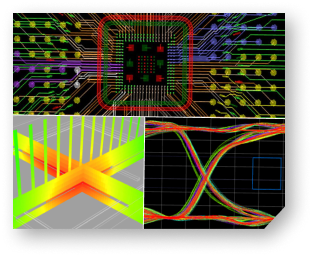
Design
- Architecture schematic layout
- Package/Board SI/PI
- Thermal & Mechanical
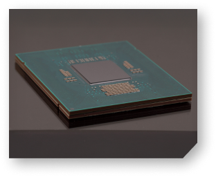
Fabrication
- 70x70, 6-2-6, 12 micron L/S
- 15/15 Std,12/12 advanced
- Build Up & Ceramic
Dicing
- Stealth Laser for PIC
- Wafer Dicing, Thinning
- Polishing and AOI of PICs
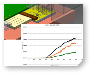
Silicon Photonics
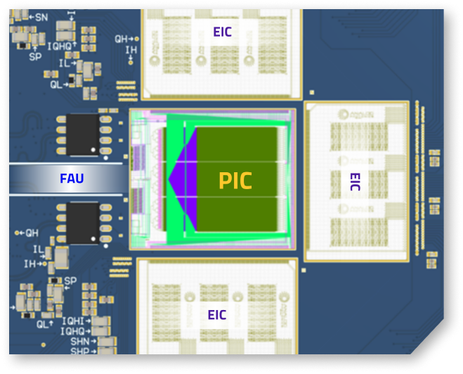
- FAU Active alignment
- Edge Coupling for 1x24 FAU
- Beam Characterization
Assembly
- +/- 0.5µm placement
- 19,000+ bumps Flip Chip
- 9 chips per SiP Module
Chiplets
- Chiplet Floor Planning
- Multi Physics optimization
- Heterogeneous Assembly
Build With The Best
The Silitronics team brings 200+ years of collective expertise in architecting designing, developing, and executing cost-effective, high-precision semiconductors and photonics packaging solutions—from initial concept to full-scale production.
Silitronics is a state-of-the-art, 20,000 sq ft automated ISO 9001 facility in San Jose, the heart of Silicon Valley, we ensure complicated process development including automated photonics active alignment, seamless scalability, and quality, consistently meeting the most demanding schedules and exceeding performance expectations.

Made in USA

Complete Turnkey Solutions

First Time Right

Prototype to Volume


Our Services Spectrum

Selected and trusted by Industry
leaders and Innovative Startups
Silicon Photonics:
Data center, Cloud
AR/VR:
Camera Sensors, Retina
AI/ML /Computing:
Cloud, 800G
LiDAR:
Driverless car, Security
Defense:
High Rel Assembly
IoT Sensors:
SiP Modules, MEMS
Medical:
In Vitro and In Vivo
Selected and trusted by Industry leaders and Innovative Startups
Silicon Photonics:
Data center, Cloud
AR/VR:
Camera Sensors, Retina
AI/ML/Computing:
Cloud, 800G
LiDAR:
Driverless car, Security
Defense:
High Rel Assembly
IoT Sensors:
SiP Modules, MEMS
Medical:
In Vitro and In Vivo
Why choose Silitronics?
20,000+ sq.ft.
State-of-the-Art
Facility:
Equipped with 10K clean rooms and fully automated assembly lines for unparalleled precision.
One-Stop Solutions
From concept to finished product, we handle it all: design, assembly, testing, and delivery.
Cutting-Edge Equipment
From ±0.5μm flip chip placement to automatic wire bonding at 20μm pitch, we deliver unmatched accuracy.
Industry-Leading TAT
8-hour turnaround for urgent prototypes and 3-day cycle times for standard builds.
Proven
Expertise
99% yield on SiP modules and 90%+ yield on RF and flex assemblies.
Why choose Silitronics?

20,000+ sq.ft.
State-of-the-Art Facility:
Equipped with 10K clean rooms and fully automated assembly lines for unparalleled precision.

One-Stop Solutions
From concept to finished product, we handle it all: design, assembly, testing, and delivery.

Cutting-Edge Equipment
From ±0.5μm flip chip placement to automatic wire bonding at 20μm pitch, we deliver unmatched accuracy.

Industry-Leading TAT
8-hour turnaround for urgent prototypes and 3-day cycle times for standard builds.

Proven Expertise
99% yield on SiP modules and 90%+ yield on RF and flex assemblies.
Case Studies and Whitepapers
Driving Innovation in LiDAR with High-Precision SiP Packaging
Flawless execution, rapid prototyping, and first-pass success for cutting-edge automotive LiDAR technology.
Download case studyAccelerating Innovation in 4K Live Streaming & Gaming Cameras
First-pass success, rapid prototyping, and precision execution for breakthrough imaging technology.
Download case studyHigh-Yield, High-Precision IC Packaging for 5G & RF Innovation
Reliable, flexible, and high-performance IC packaging solutions, ensuring uninterrupted supply and exceptional quality.
Download case studyBreaking the Bottleneck: Silicon Photonics and the Next Leap in High-Speed Data Transfer
How Silicon Photonics is revolutionizing AI clusters, HPC, and next-gen computing by overcoming electrical interconnect limitations.
Download case studyHeterogeneous Integration: Unlocking Next-Gen Semiconductor Performance Beyond Moore's Law
How advanced packaging techniques like 2.5D, 3D IC, and Chiplet integration are driving the semiconductor industry forward.
Download case studySustainable Semiconductor Packaging: Reducing Power, Heat, and Waste in Next-Gen Electronics
How eco-friendly materials, energy-efficient designs, and advanced photonics are driving sustainability in semiconductor manufacturing.
Download case studyInterested in our end-to-end advanced semiconductor and photonics (PIC) packaging solutions?
Get in touch


