


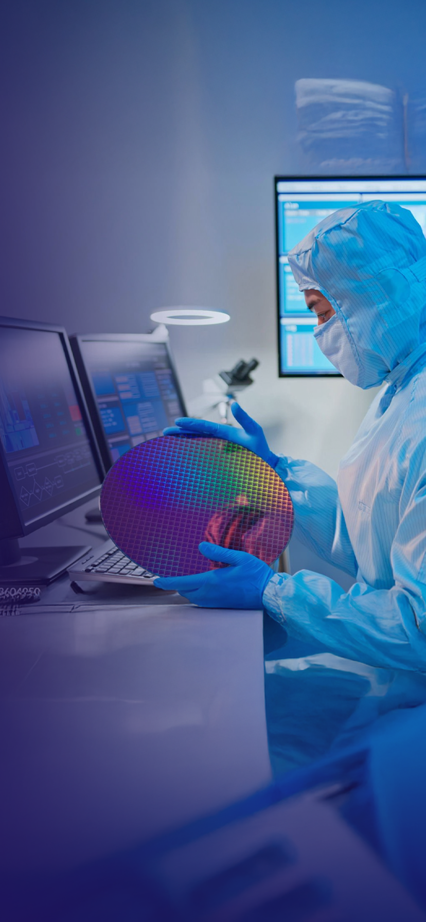

Advanced Semiconductor and Silicon Photonics Packaging Services
From Silicon Photonics to Advanced Semiconductor Design, Fabrication, and Assembly, we deliver end-to-end advanced semiconductor and PIC packaging solutions with unmatched expertise.
Our current edge equipment and facilities coupled with engineering expertise ensures seamless integration, high performance, and first-pass success, empowering breakthroughs in AI, HPC, and next-gen connectivity. Experience engineering excellence that drives the future of innovation.

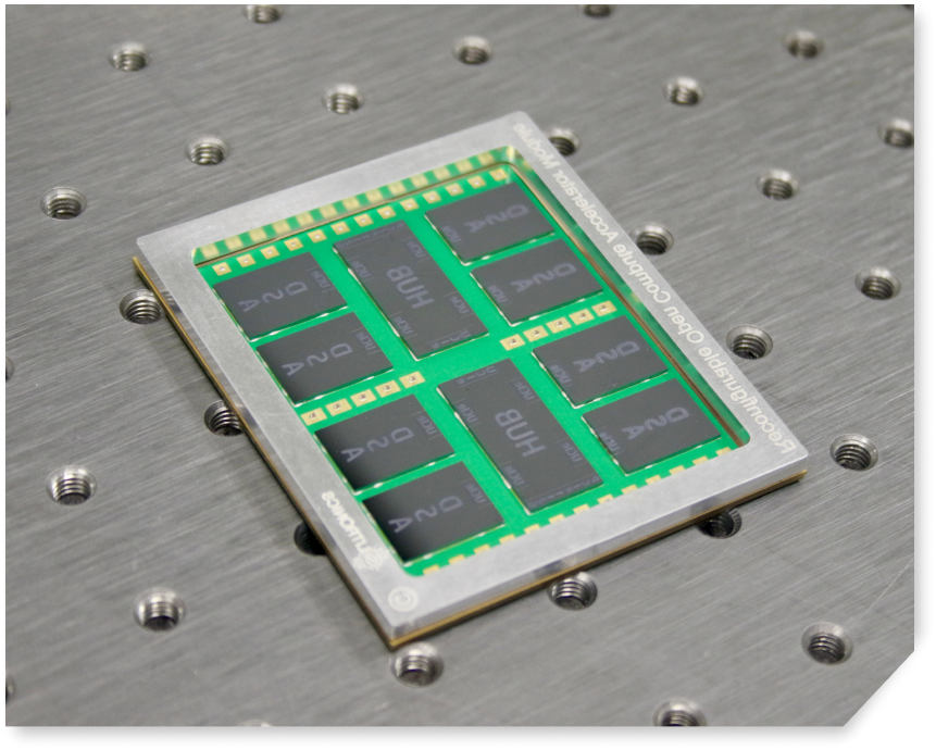
Breakthrough Chiplet Integration for Scalable, Next-Gen Systems
Silitronics empowers the future of electronics with advanced chiplet integration, merging diverse dies on precision-engineered interposers for optimal signal, power, and thermal performance. Our expertise in modular floor planning and heterogeneous assembly accelerates high-bandwidth, low-latency connectivity that is essential for AI, HPC, and 5G+. From concept design to rigorous validation, Silitronics helps customers bring complex systems to market faster, smarter, and more reliably.
LEARN MORE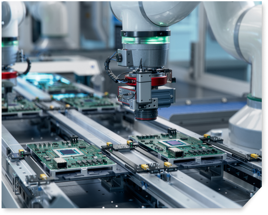
Seamless Assembly for High-Precision Semiconductor & Photonic Packaging
Our cutting-edge assembly expertise ensures precise chip-to-package integration with industry-leading sub-micron active alignment, high-density interconnects, and heterogeneous integration. We specialize in complex optical and electronic assemblies for AI accelerators, 5G networks, and next-gen computing, delivering high-reliability solutions that optimize performance and reduce time to market.
LEARN MORE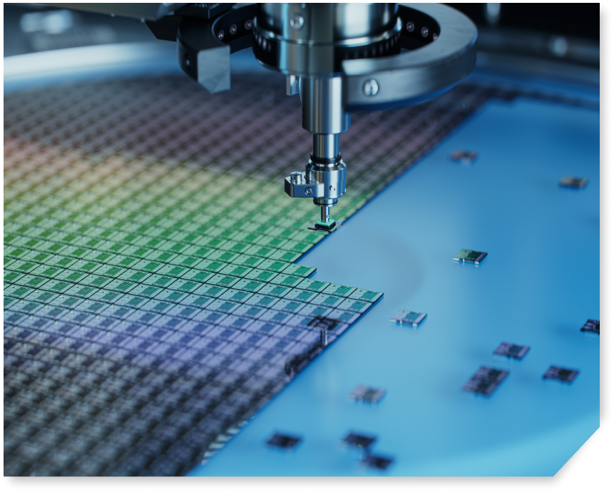
High-Precision Wafer Dicing
We deliver advanced wafer dicing using precision blade and laser technologies to ensure clean die separation with minimal chipping. Optimized for high yield and low particle contamination, our dicing supports next-gen semiconductor packaging and performance.
LEARN MORE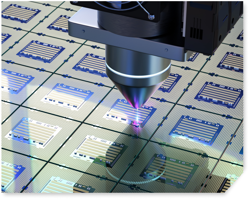
Fabrication for Advanced
Semiconductor & Photonic Packaging
Our state-of-the-art fabrication facility delivers high-precision multi-layer substrates tailored for AI, HPC, and Silicon Photonics. With expertise in organic and ceramic substrates, fine-pitch interconnects, and high-density integration, we ensure superior reliability, scalability, and manufacturing excellence. From prototypes to high-volume production, we bring innovation to life with precision.
LEARN MORE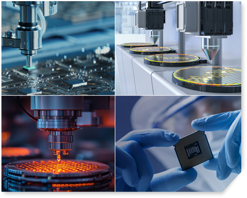
Precision-Driven Design for
Next-Gen Semiconductor &
Photonic Packaging
From concept to layout, our advanced design expertise ensures seamless integration of chips, substrates, and interconnects. We optimize signal integrity, power efficiency, and thermal performance to meet the demands of AI accelerators, quantum computing, and high-speed photonic systems. With deep engineering insights, we design scalable, high-reliability solutions for the future.
LEARN MORE
Powering the Future at the
Speed of Light with Photonics
Silicon Photonics is transforming high-speed computing, AI clusters, and next-gen data transfer. Our expertise in sub-micron active alignment, optical integration, and high-bandwidth packaging ensures low-latency, energy-efficient performance. From LiDAR to AI-driven interconnects, we deliver cutting-edge photonics solutions that push the limits of speed, scalability, and efficiency.
LEARN MORE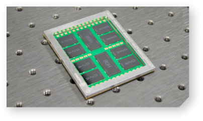
Breakthrough Chiplet Integration for Scalable, Next-Gen Systems
Silitronics empowers the future of electronics with advanced chiplet integration, merging diverse dies on precision-engineered interposers for optimal signal, power, and thermal performance. Our expertise in modular floor planning and heterogeneous assembly accelerates high-bandwidth, low-latency connectivity that is essential for AI, HPC, and 5G+. From concept design to rigorous validation, Silitronics helps customers bring complex systems to market faster, smarter, and more reliably.
LEARN MORESeamless Assembly for High-Precision Semiconductor & Photonic Packaging
Our cutting-edge assembly expertise ensures precise chip-to-package integration with industry-leading sub-micron active alignment, high-density interconnects, and heterogeneous integration. We specialize in complex optical and electronic assemblies for AI accelerators, 5G networks, and next-gen computing, delivering high-reliability solutions that optimize performance and reduce time to market.
LEARN MOREHigh-Precision Wafer Dicing
We deliver advanced wafer dicing using precision blade and laser technologies to ensure clean die separation with minimal chipping. Optimized for high yield and low particle contamination, our dicing supports next-gen semiconductor packaging and performance.
LEARN MOREFabrication for Advanced Semiconductor & Photonic Packaging
Our state-of-the-art fabrication facility delivers high-precision multi-layer substrates tailored for AI, HPC, and Silicon Photonics. With expertise in organic and ceramic substrates, fine-pitch interconnects, and high-density integration, we ensure superior reliability, scalability, and manufacturing excellence. From prototypes to high-volume production, we bring innovation to life with precision.
LEARN MORE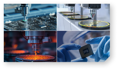
Precision-Driven Design for Next-Gen Semiconductor & Photonic Packaging
From concept to layout, our advanced design expertise ensures seamless integration of chips, substrates, and interconnects. We optimize signal integrity, power efficiency, and thermal performance to meet the demands of AI accelerators, quantum computing, and high-speed photonic systems. With deep engineering insights, we design scalable, high-reliability solutions for the future.
LEARN MORE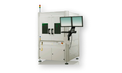
Powering the Future at the Speed of Light with Photonics
Silicon Photonics is transforming high-speed computing, AI clusters, and next-gen data transfer. Our expertise in sub-micron active alignment, optical integration, and high-bandwidth packaging ensures low-latency, energy-efficient performance. From LiDAR to AI-driven interconnects, we deliver cutting-edge photonics solutions that push the limits of speed, scalability, and efficiency.
LEARN MORECase Studies
Flawless execution, rapid prototyping, and first-pass success for cutting-edge automotive LiDAR technology.
Flawless execution, rapid prototyping, and first-pass success for cutting-edge automotive LiDAR technology.
Download case studyAccelerating Innovation in 4K Live Streaming & Gaming Cameras
First-pass success, rapid prototyping, and precision execution for breakthrough imaging technology.
Download case studyHigh-Yield, High-Precision IC Packaging for 5G & RF Innovation
Reliable, flexible, and high-performance IC packaging solutions, ensuring uninterrupted supply and exceptional quality.
Download case studyInterested in our end-to-end advanced semiconductor and photonics (PIC) packaging solutions?